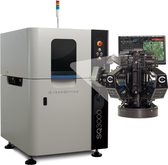
Speed your semiconductor processes with WaferSense® and ReticleSense® measurement devices

When you need the most efficient and effective measurement devices for semiconductor tool set-up and maintenance processes, count on CyberOptics, the global market leader in wireless semiconductor measurement devices for chamber gapping, leveling, wafer handoff teaching, vibration and airborne particle measurement.
Semiconductor fabs and OEMs value the accuracy, precision and versatility of the WaferSense and ReticleSense measurement portfolio to enable improvements in fab yields and equipment uptime.
Mr. Yukinobu Hayashi—Field Application Engineer, CyberOptics— shared a poster presentation at the PhotoMask Japan Conference recently. He highlighted the 10X time savings using the ReticleSense APSR Quartz for identifying and resolving particle issues compared to alternate solutions.
At the recent CSManTech Conference, Mr. Allyn Jackson shared process improvement results in semiconductor manufacturing environments using WaferSense® and ReticleSense® Wireless Measurement Devices. Visit our site for more information about the entire semiconductor sensor portfolio that can significantly improve yields and tool uptime.